Chiral twisted van der Waals Nanowires
(Nature 570, 354-357 (2019), DOI: 10.1038/s41586-019-1147-x)
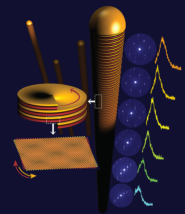
Van der Waals heterostructures with small misalignment between adjacent layers (‘interlayer twist’) are of interest because of electronic structure and correlation phenomena (such as superconductivity) that are determined by both the atomic lattice and long-range superlattice potentials arising in interlayer moiré patterns. Previously, such twisted heterostructures have involved a single planar interface between layers isolated by exfoliation and micromechanically stacked in the desired relative orientation. We demonstrated a class of materials—van der Waals nanowires of layered crystals—in which a tunable interlayer twist evolves naturally during synthesis. In vapour–liquid–solid growth, nanowires of germanium(ii) sulfide, an anisotropic layered semiconductor, crystallize with layering along the wire axis and have a strong propensity for forming axial screw dislocations. Nanometre-resolved electron diffraction shows that Eshelby twist, induced by a torque on the ends of a cylindrical solid due to the stress field of an axial dislocation, causes a chiral structure in the van der Waals nanowires. The in-plane germanium sulfide crystal axes progressively rotate along the wire, and germanium sulfide layers in adjacent turns of the helix naturally form a moiré pattern because of their interlayer twist. The axial rotation and the twist are tunable by varying the nanowire thickness. Combined electron diffraction and cathodoluminescence spectroscopy show the correlation between the interlayer twist and locally excited light emission that is due to progressive changes in the lattice orientation and in the interlayer moiré registry along the nanowires. The findings demonstrate a step towards scalable fabrication of van der Waals structures with defined twist angles, in which interlayer moiré patterns are realized along a helical path on a nanowire instead of a planar interface. Link to UNL Press Release.
Self-organized twist-heterostructures via aligned van der Waals epitaxy and solid-state transformations
(Nature Communications 10, 5528 (2019), DOI: 10.1038/s41467-019-13488-5)
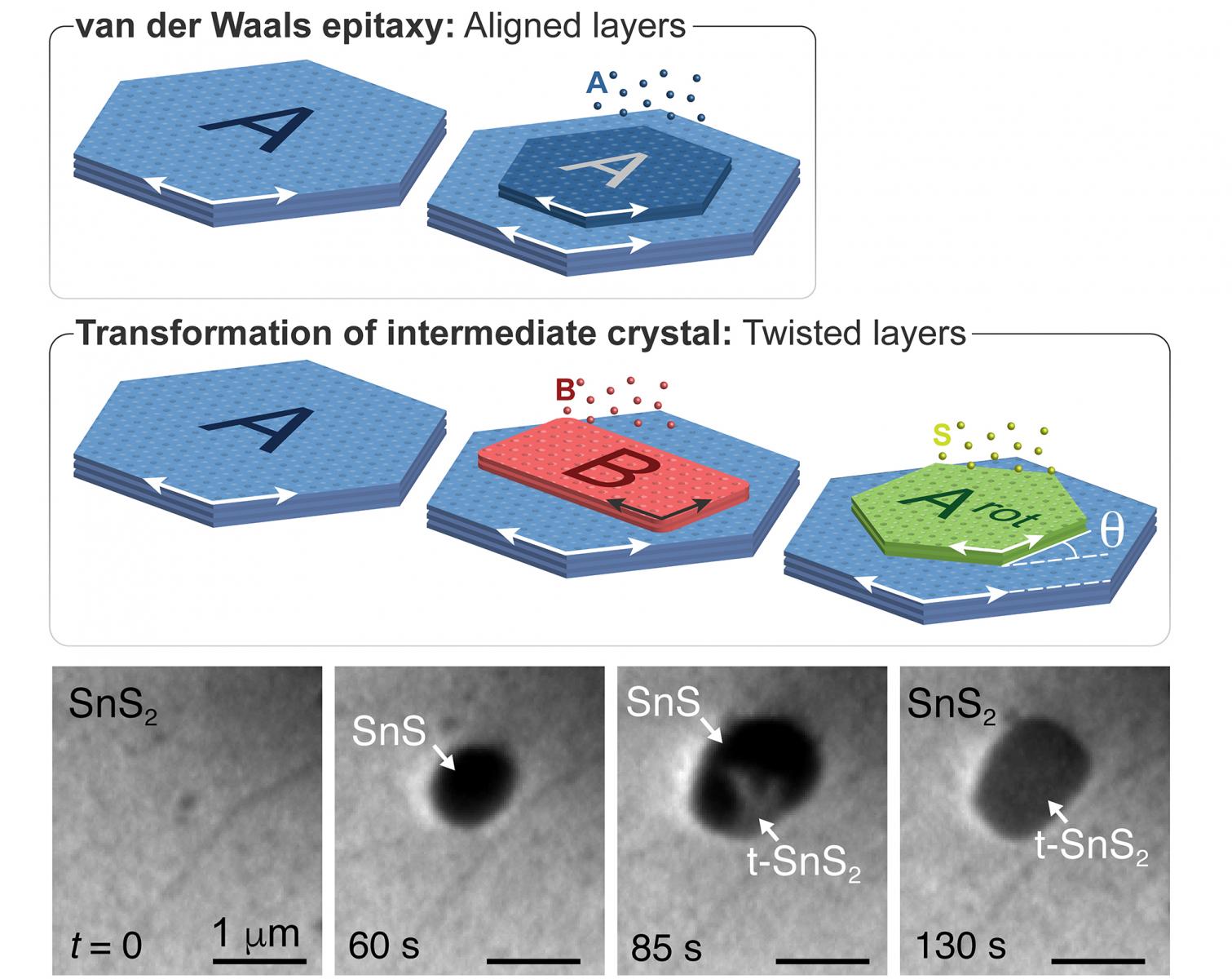

Vertical van der Waals (vdW) heterostructures of 2D crystals with defined interlayer twist are of interest for band-structure engineering via twist moiré superlattice potentials. To date, twist-heterostructures have been realized almost exclusively by micromechanical stacking. Direct synthesis is hindered by the tendency toward equilibrium stacking without interlayer twist. We demonstrated that growing a 2D crystal with fixed azimuthal alignment to the substrate followed by transformation of this intermediate enables a potentially scalable synthesis of twisted heterostructures. Microscopy during growth of ultrathin orthorhombic SnS on trigonal SnS2 shows that vdW epitaxy yields azimuthal order even for non-isotypic 2D crystals. Excess sulfur drives a spontaneous transformation of the few-layer SnS to SnS2, whose orientation – rotated 30° against the underlying SnS2 crystal – is defined by the SnS intermediate rather than the substrate. Preferential nucleation of additional SnS on such twisted domains repeats the process, promising the realization of complex twisted stacks by bottom-up synthesis. These results define a new paradigm for van der Waals epitaxy - and possibly more generally for thin film growth - in which the orientation of a newly added layer is no longer defined by the underlying substrate lattice but is inherited through a solid-state transformation from an intermediate crystal phase. Link to UNL Press Release.
Wrap-around core-shell heterostructures of layered crystals
(Advanced Materials 31, 1902166 (2019), DOI: 10.1002/adma.201902166)
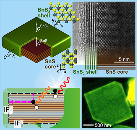
Engineered heterostructures create new functionality by integrating dissimilar materials. Combining different 2D crystals naturally produces two distinct classes of heterostructures, vertical van der Waals (vdW) stacks or 2D sheets bonded laterally by covalent line interfaces. When joining thicker layered crystals, the arising structural and topological conflicts can result in more complex geometries. Phase separation during one‐pot synthesis of layered tin chalcogenides spontaneously creates core–shell structures in which large orthorhombic SnS crystals are enclosed in a wrap‐around shell of trigonal SnS2, forcing the coexistence of parallel vdW layering along with unconventional, orthogonally layered core–shell interfaces. Measurements of the optoelectronic properties establish anisotropic carrier separation near type II core–shell interfaces and extended long‐wavelength light harvesting via spatially indirect interfacial absorption, making multifunctional layered core–shell structures attractive for energy‐conversion applications. Link to DOE-BES Highlight.
Growth mechanisms of anisotropic layered group IV chalcogenides on van der Waals substrates for energy conversion applications
(ACS Applied Nano Materials 1, 3026 (2018), DOI: 10.1021/acsanm.8b00660)
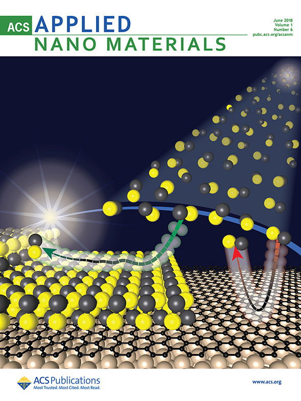
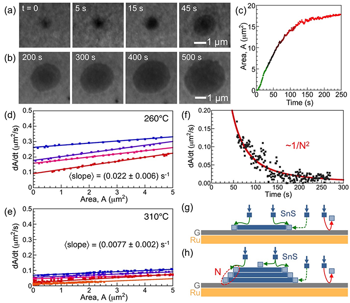
Two-dimensional group IV monochalcogenide semiconductors (SnX, GeX; X = S, Se) are of fundamental interest due to their anisotropic crystal structure and predicted unique characteristics such as large exciton binding energies and multiferroic order possibly up to above room temperature. Whereas growth on reactive supports produces mostly standing flakes, deposition on van der Waals (vdW) substrates can yield basal-plane oriented layered crystals. But so far, this approach invariably resulted in flakes that are several atomic layers thick and the synthesis of monolayers has remained elusive. We used in-situ microscopy during molecular beam epitaxy of SnS on graphite and graphene to establish the origin of this predominant multilayer growth. The enhanced reactivity of group IV chalcogenide layers causes adsorption of precursor molecules primarily on the initial SnS nuclei instead of the vdW support. On graphite, this unusual imbalance in the material supply is the primary cause for fast vertical growth. Experiments on graphene/Ru(0001) suggest increased adsorption on the vdW substrate, which enables enhanced lateral SnS growth. The obtained fundamental insight provides a basis for identifying conditions for the scalable synthesis of single-layer group IV monochalcogenides, and guides the growth of high-quality multilayer films of interest for applications in energy conversion, optoelectronics, and thermoelectrics.
In situ electron microscopy of plasmon-mediated nanocrystal synthesis
(Journal of the American Chemical Society 139, 6771 (2017), DOI: 10.1021/jacs.7b03668; see also the JACS spotlight: http://pubs.acs.org/doi/10.1021/jacs.7b06510)
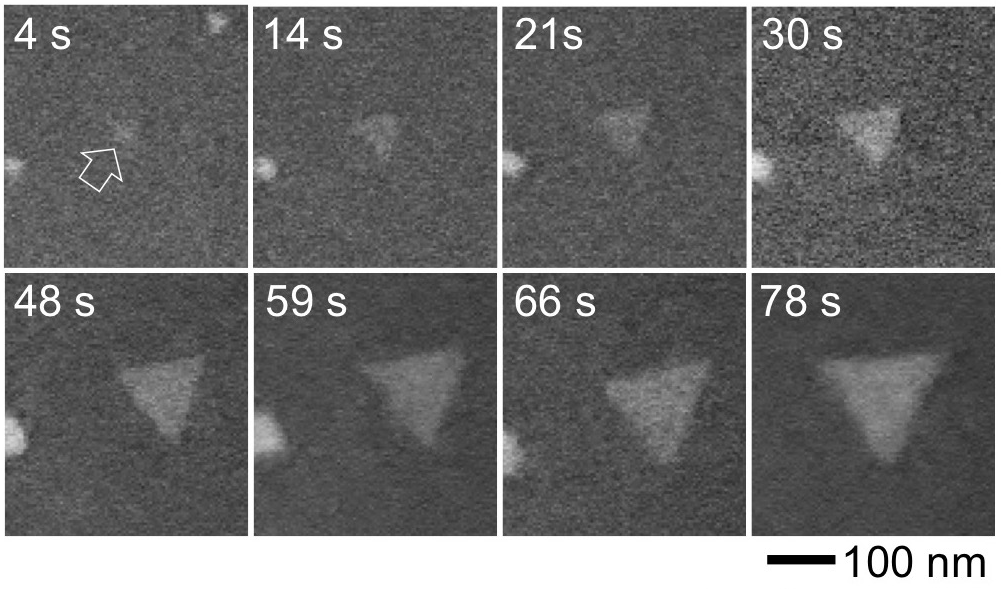
Chemical processes driven by nonthermal energy (e.g., visible light) are attractive for future approaches to energy conversion, synthesis, photocatalysis, etc. The growth of anisotropic metal nanostructures mediated by excitation of a localized surface plasmon resonance (LSPR) is a prototype example of such a reaction. Important aspects, notably the growth mechanism and a possible role of plasmonic “hot spots” within the metal nanostructures, remain poorly understood. We used in situ electron microscopy to stimulate and image the plasmon-mediated growth of triangular Ag nanoprisms in solution. The quantification of the time-dependent evolution of the lateral size and thickness of the nanoprisms, enabled by nanometer-scale real-time microscopy in solution, shows a transition from an early stage of uniform Ag0 incorporation exclusively in the prism side facets to a size regime with accelerated growth in thickness. Differences in attachment rate at this advanced stage correlate with local plasmonic field enhancements, which allows determining the range over which charge carriers transferred from plasmonic hot spots can drive chemistry. Such data support the development of nonthermal chemical processes that depend on plasmonic light harvesting and the transfer of nonequilibrium charge carriers.
Electron-beam induced transformations of layered tin dichalcogenides
(Nano Letters 16, 4410 (2016), DOI: 10.1021/acs.nanolett.6b01541)
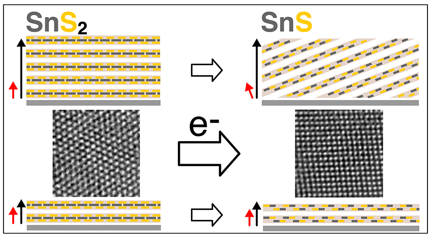
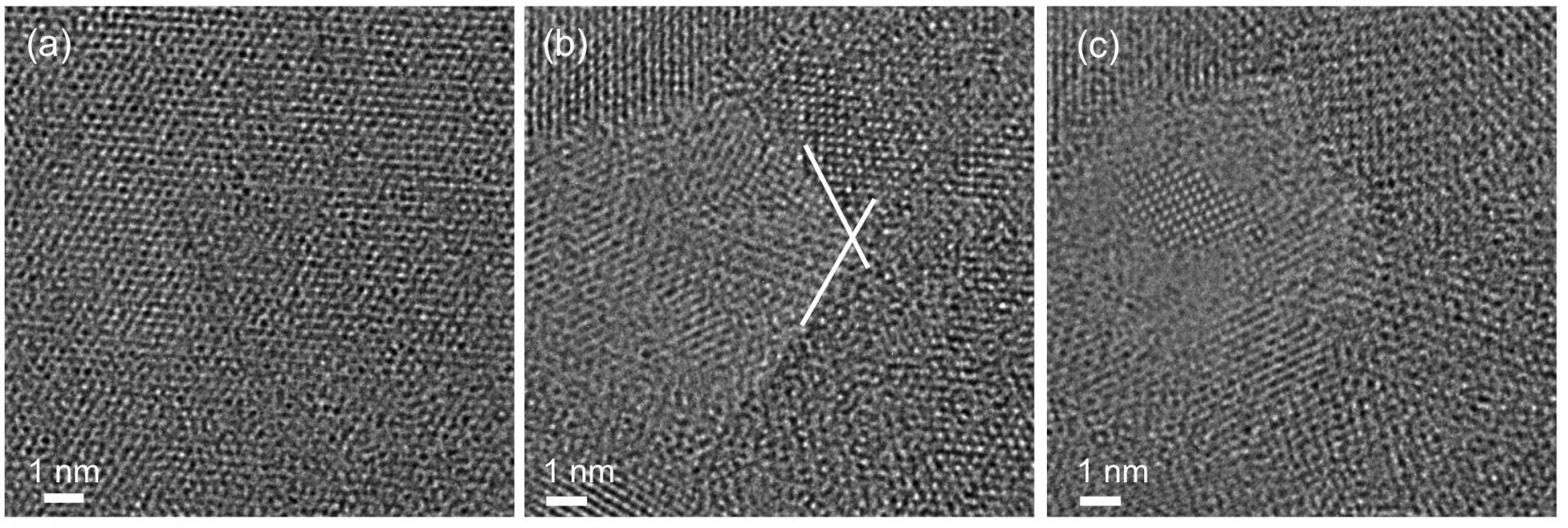

By combining high-resolution transmission electron microscopy and associated analytical methods with first-principles calculations, we studied the behavior of layered tin dichalcogenides under electron beam irradiation. We demonstrated that the controllable removal of chalcogen atoms due to electron irradiation gives rise to transformations in the atomic structure of Sn–S and Sn–Se systems so that new phases with different properties can be induced. In particular, rhombohedral layered SnS2 and SnSe2 can be transformed via electron beam induced loss of chalcogen atoms into highly anisotropic orthorhombic layered SnS and SnSe. A striking dependence of the layer orientation of the resulting SnS—parallel to the layers of ultrathin SnS2 starting material, but slanted for transformations of thicker few-layer SnS2—is rationalized by a transformation pathway in which vacancies group into ordered S-vacancy lines, which convert via a Sn2S3 intermediate to SnS. Absence of a stable Sn2Se3 intermediate precludes this pathway for the selenides, hence SnSe2 always transforms into basal plane oriented SnSe. Our results provide microscopic insights into the transformation mechanism and show how irradiation can be used to tune the properties of layered tin chalcogenides for applications in electronics, catalysis, or energy storage.
In situ microscopy of the self-assembly of branched nanocrystals in solution
(Nature Communications 7, Article number:11213 (2016), doi:10.1038/ncomms11213)
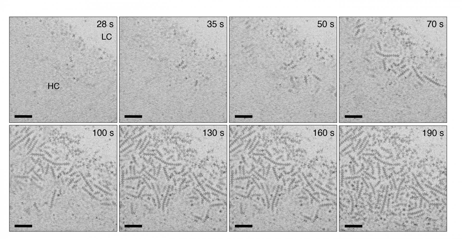
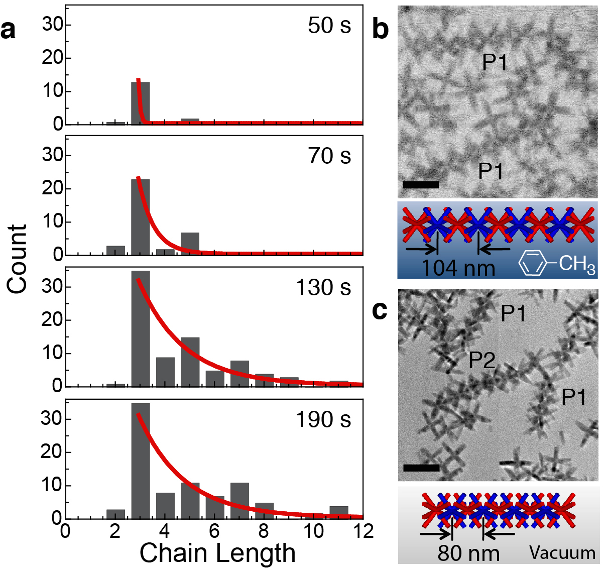
Solution-phase self-assembly of nanocrystals into mesoscale structures is a promising strategy for constructing functional materials from nanoscale components. Liquid environments are key to self-assembly since they allow suspended nanocrystals to diffuse and interact freely, but they also complicate experiments. Real-time observations with single-particle resolution can have transformative impact on our understanding of nanocrystal self-assembly. We used real-time in situ imaging by liquid-cell electron microscopy to elucidate the nucleation and growth mechanism and properties of linear chains of octapod-shaped nanocrystals in their native solution environment. Statistical mechanics modelling based on these observations and using the measured chain-length distribution clarifies the relative importance of dipolar and entropic forces in the assembly process and gives direct access to the interparticle interaction. Our results suggest that monomer-resolved in situ imaging combined with modelling can provide unprecedented quantitative insight into the microscopic processes and interactions that govern nanocrystal self-assembly in solution. Link to UNL Press Release.